In the relentless pursuit of miniaturization and functionality, modern electronics demand materials that defy traditional categories. They require the electrical and thermal prowess of metals combined with the thinness, lightness, and flexibility of polymers. This is precisely where Vacuum Deposited Copper Film emerges as a transformative solution. This advanced material is engineered by depositing ultra-pure copper onto high-performance flexible substrates like BOPET (Biaxially Oriented Polyethylene Terephthalate) or BOPI (Biaxially Oriented Polyimide) using sophisticated Physical Vapor Deposition (PVD) technology. The result is a hybrid marvel: a film that retains the excellent physical, chemical, and dimensional stability of its base while gaining the superior conductive and thermal properties of solid metal. This article delves into the production, unparalleled advantages, and critical applications of Vacuum Deposited Copper Film, establishing it as a cornerstone material for next-generation electronic design.
Section 1: The Science of Synthesis – How Vacuum Deposited Copper Film is Made
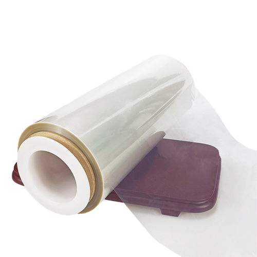
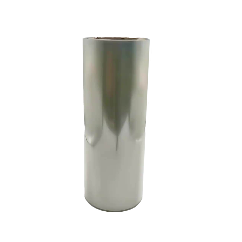
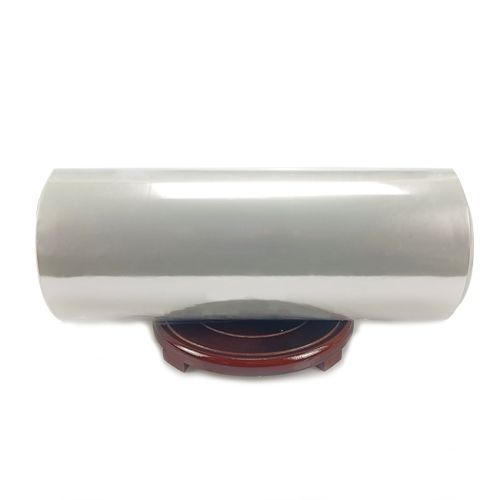
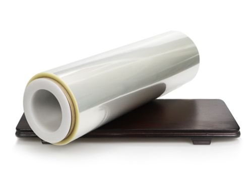
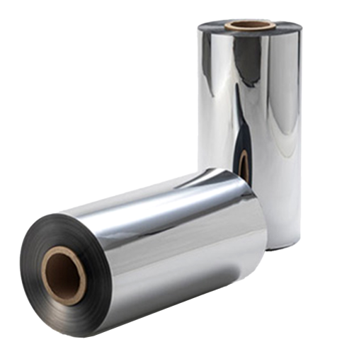
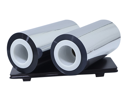
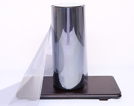
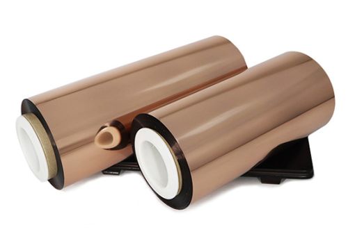
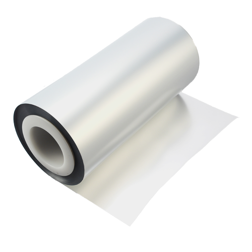
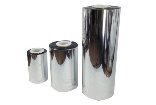
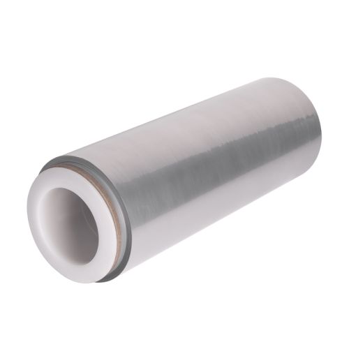
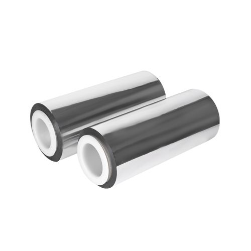
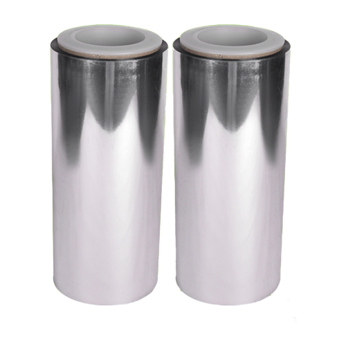
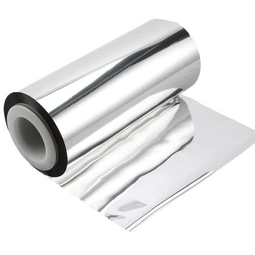
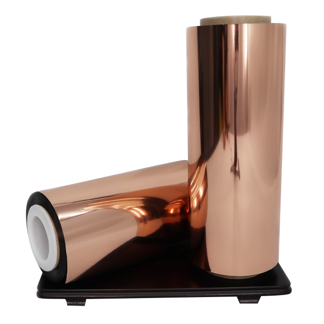
The exceptional quality of Vacuum Deposited Copper Film stems from its precise and controlled manufacturing process.
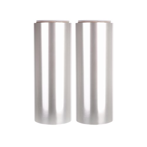
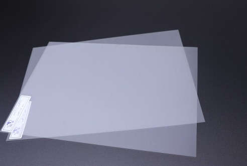
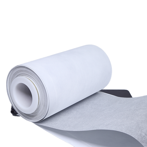
- The Foundation: High-Stability Substrates: The process begins with selecting a base film known for its robustness. BOPET offers excellent tensile strength, chemical resistance, and thermal stability up to 120°C. For more demanding environments, BOPI (Kapton-like films) is chosen for its exceptional thermal resistance (often exceeding 200°C) and outstanding dimensional stability. This choice determines the film’s performance under stress and heat.
- The Core Technology: Physical Vapor Deposition (PVD): The substrate is fed into a state-of-the-art roll-to-roll vacuum coater. Inside a high-vacuum chamber, a source of 99.999% pure copper is energized, typically through processes like electron-beam evaporation or sputtering. This causes copper atoms to be ejected from the source.
- Creating the Metallic Layer: In the vacuum environment, these vaporized copper atoms travel unimpeded and condense uniformly onto the cool surface of the moving substrate. By meticulously controlling parameters like vacuum pressure, deposition rate, and web speed, manufacturers can produce a copper layer of exceptional purity, uniformity, and adhesion, with thicknesses controllable from a few nanometers to micrometers.
Section 2: Unmatched Advantages: Why Designers Choose This Film
This unique fabrication method endows Vacuum Deposited Copper Film with a compelling set of properties that pure metals or conventional laminates cannot match.
- Superior Electrical Conductivity: The high-purity, continuous copper layer provides excellent surface conductivity. This enables efficient current carrying and low-resistance pathways, making it ideal for circuits, electrodes, and antennas.
- Exceptional Thermal Conductivity: Copper is one of nature’s best thermal conductors. This film effectively draws heat away from hot spots (like LEDs, CPUs, or power components), spreading it across a larger area for dissipation, which is crucial for device reliability and longevity.
- Inherent Flexibility and Durability: Unlike brittle copper foil, the polymer substrate allows the film to be repeatedly bent, folded, or flexed without cracking the conductive layer. It exhibits excellent resistance to fatigue, making it perfect for dynamic applications or flexible assemblies.
- Outstanding Dimensional Stability: Both BOPET and BOPI substrates resist stretching, shrinking, and warping under thermal and mechanical stress. This ensures that circuits printed on the film maintain their precise alignment and performance, even during soldering or in varying environmental conditions.
- Lightweight and Thin Profile: It provides metallic functionality at a fraction of the weight and thickness of traditional copper sheets or cladded laminates, enabling lightweight and compact device designs.
- Strong Adhesion: The PVD process creates a clean, atomic-level bond between the copper and the substrate, ensuring the metal layer remains firmly attached during processing, soldering, and use.
Section 3: Diverse Applications Across Industries
The combination of conductivity, flexibility, and stability opens doors to numerous advanced applications.
- Electronics Thermal Management: Used as a heat spreader in smartphones, tablets, and LEDs. It is integrated into displays or PCB assemblies to draw heat away from critical components, preventing overheating and performance throttling.
- Flexible Circuits and Electrodes: Serves as a key material for flexible printed circuits (FPCs), membrane switches, and sensors. Its ability to maintain conductivity while bending is essential for wearable electronics, medical devices, and flexible displays.
- Electromagnetic Interference (EMI) Shielding: The conductive copper layer acts as a highly effective Faraday cage, shielding sensitive electronic components from external EMI and preventing the device’s own emissions from causing interference. It is often laminated or adhesively applied as a critical shield in cable wraps, enclosures, and gaskets.
- RFID and Smart Labels: Provides the conductive antenna inlays for UHF/HF RFID tags and NFC tags. The process allows for precise, high-volume patterning of efficient, low-cost antennas on flexible rolls.
- Functional Adhesives and Tapes: When laminated with conductive or non-conductive adhesives, it becomes a conductive transfer tape or EMI shielding tape. These are used for Z-axis electrical connections, grounding, or creating shielded compartments within devices.
- Advanced Security and Anti-Counterfeiting: The film can be intricately patterned, die-cut, and integrated into security labels, holograms, and passports. The specific electrical signature or intricate metallic pattern is extremely difficult to replicate, providing a high level of security.
Conclusion
Vacuum Deposited Copper Film is more than just a material; it is a fundamental enabler of modern electronic innovation. By seamlessly merging the world of high-purity metals with advanced polymer science, it delivers a unique set of properties—lightweight conductivity, reliable thermal management, robust flexibility, and effective EMI shielding—that are essential for the devices of today and tomorrow. From the smartphone in your pocket to the critical systems in electric vehicles and medical equipment, this film plays a vital, often unseen role. For engineers and product designers pushing the boundaries of what’s possible, understanding and specifying Vacuum Deposited Copper Film is key to creating products that are more powerful, reliable, and compact.